Nano- and Micro- Engineered Materials for the Reduction of SEE
Materials with surface architecture on the nano and micro scale are engineered for the reduction of secondary electron emission. Micro cavities are shown to trap emitted electrons, reducing the overall secondary electron yield from the material with respect to flat surfaces. Challenges in analyzing these materials include avoiding enhancements of strong electric field emission due to irregularities on the complex surfaces which may occur for high discharge voltage operations, typical of high Isp applications.
Ultrananocrystalline Diamond Coatings (UNCD)
Effects of electron field emission is studied for nitrogen incorporated and undoped UNCD coatings. Grain sizes for these materials are on the nm order, and have been shown to have exceptional field emission properties. Experiments are carried out for samples of varying grain size by immersion in a low temperature plasma using specially designed holders probe-collectors. Biasing the plasma-facing side of the holder with respect to the plasma it is possible to measure charged particle emission (field emission, secondary electron or thermionic emission). Due to screening of closely spaced grains and a larger sheath size (~ 102μm), field enhacement has been found to be negligible.
Carbon Velvet
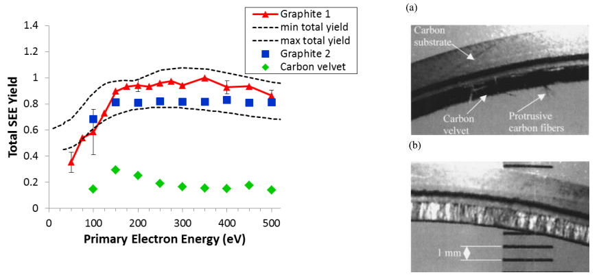
Carbon velvet is a high aspect ratio material made of carbon fibers bonded on carbon substrates. Fibers are 0.5-3.0mm in length present interfiber cavities with aspect ratio of ~102. This material has been shown to suppress both ion-induced and electron-induced secondary electron emissions for Hall thruster electrodes as well as being highly sputter resistant. Carbon velvet has been used to coat segmented electrodes on the 2kW Hall thruster to analyze the reduction of SEE and therefore reduction of electron energy losses at the channel walls. Methods for measuring SEE from carbon velvet materials include Auger electron spectroscopy and scanning electron microscopy.
Boron Nitride Ceramic Materials
Secondary electron yield of boron nitride and quartz dielectric materials is also studied as a function of primary electron beam energy (50-120eV) and sample temperature. SEE properties of boron nitride ceramic grade M26 have been shown to be reduced with an increase of the sample from room temperature to 300-400oC. Experiments are conducted at the Surface Science and Technology Laboratory at PPPL.
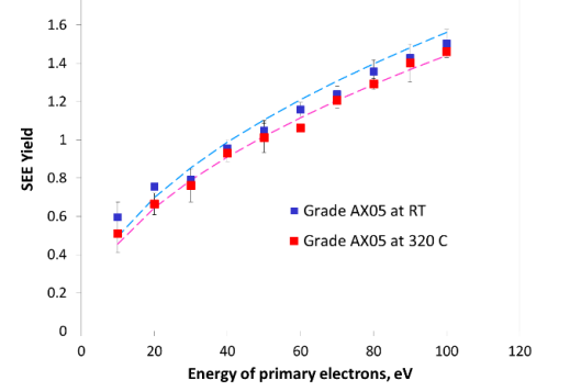
SEE yield for BN grades at room temperature and 320oC.