Secondary Electron Emission Properties of Plasma-Facing Surfaces and Materials
Yield of electron induced secondary electron emission is one of the key parameters of dielectric materials. It determines the development of electron avalanches, which are responsible on the surface flashover of insulators. Secondary electron emission (SEE) governs the process of electrical charging of spacecrafts, which can lead to electrical breakdowns. Secondary electron emission affects plasma discharges through plasma-wall interaction, which is in great importance for plasma propulsion devices. In particular, in Hall thrusters the potential drops on the sheath and presheath, and, as a result, the electron losses on the channel walls, depend strongly on the yield of secondary electron emission (SEE) from the wall material. The distribution of the electron temperature along the thruster channel is also affected by SEE. Segmented electrodes made of a material with different secondary emission properties have been shown to affect the potential distribution in the thruster channel, which, in turn, might cause the observed 20% reduction of the plasma plume divergence. Thus, it is of great importance to describe precisely the yield of SEE from thruster wall materials, induced by plasma electrons with energies of a few tens of electron-volts.
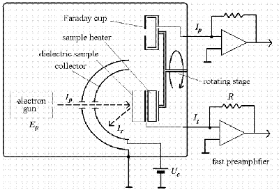
Sketch of the Experimental Setup
In spite of actuality, there is still lack of systematic data on secondary electron emission from dielectrics, especially at low energies of incident electrons. The experimental setup developed at HTX group in PPPL realizes the pulsed approach to the direct measurements of electron induced SEE from dielectrics. The primary electron beam with the current of a few hundreds of nanoamperes and the electron energy of 6-1000 eV is modulated by pulses of 0.1-3 ms. The primary current is measured by a Faraday cup, mounted together with the sample holder on a rotation stage. Samples can be heated up to 800 °C.
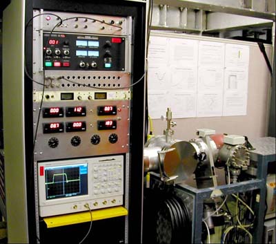
Secondary Electron Emission Setup Exterior